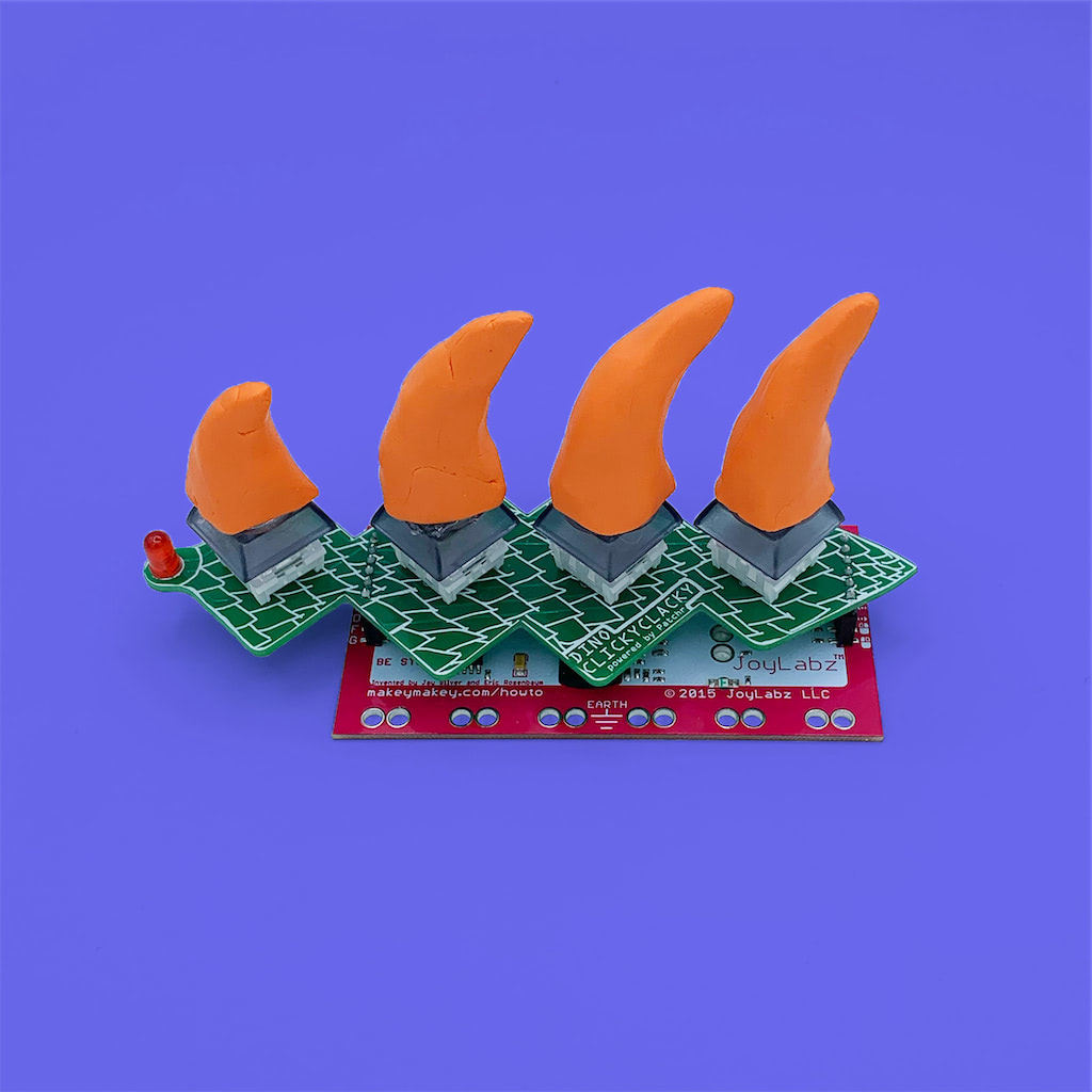
Click Clack Backpack for Makey Makey
Lesson Overview#
In this lesson you'll learn how to design and build a custom keyboard backpack for your Makey Makey.
Key Topics & Concepts
- Makey Makey backpack
- Mechanical keys
Supporting Topics and Concepts
- LED as an indicator
- Reference designators
Important Note#
This lesson does not include a Makey Makey and is compatible with v.1.4 and higher only.
If you don't have the right version, head over to the Makey Makey website and pick one up — you'll need it for the backpack to work.

What is a Makey Makey Backpack?#
A Makey Makey Backpack is an accessory board for your Makey Makey that extends its hardware capabilities.
Using the Makey Makey key remapping software, you'll be able to assign those keys to be used by your computer.
The backpack that you will design in this lesson adds four mechanical keys, which you will be able to use in the custom software that you write.
Bill of Materials#

Before you dive into designing your backpack, it's wise to familiarize yourself with all the electronic components involved in the lesson.
Most of the components will be familiar to you if you've taken another Patchr lessons or if you've learned electronics with breadboarding.
But if you're completely new to electronics, that's OK too. The table below provides an overview of the bill of materials (called BOM for short, and rhymes with Tom).
Each entry in the BOM has a component name, the Patchr symbol that represents the component in the design software, and links to the Patchr glossary that cover each component in depth.
| Component Name | Patchr Symbol | Schematic Symbol |
|---|---|---|
| Red LED (x1) |  |  |
| Mechanical Keys (x4) |  |  |
| Makey Makey Header Socket |  |
Of course, there's one component in the BOM that isn't designed yet, so it's not in the list. That's the printed circuit board — aka the PCB. More on that component in a bit.
Now that you're familiar with the entire bill of materials, it's time to review the schematic and learn how the circuit works.
How the Circuit Works#

The Click Clack Backpack's circuit is made up of four mechanical keys and one red LED, plus header pins that allow the backpack to connect to your Makey Makey.
Each of the header pins on the backpack connects to a specific pins on the Makey Makey. So when a key is pressed on the backpack, it sends an electrical signal that the Makey Makey can understand.
Board Shape Design#
Click Clack Backpack customization begins with the board shape. In this step you can create a custom board shape using the built-in drawing tools found in the left toolbar or you can upload a custom SVG file from your computer using the toolbar on the right of the screen.
Regardless of which customization tool you decide to use, there are a few things to keep in mind while designing.
The custom board cannot exceed 100x100mm. The design window shows this with light red shading and OUT OF BOUNDS text. If your shape exceeds the boundary, you will get an error notification and be unable to advance to the next step in the design process.
The white area inside the red shading denotes the space you have to work with for your board shape.
The dotted red lines that make a small rectangle indicate the minimum size your board can be — if you made your board any smaller than this area, you would not be able to layout your components or route them.
Zooming & Moving#
Zooming in and out can be done with the icons in the left toolbar or by using your mouse's scroll wheel.
To reorient your design workspace, hold the right mouse button down and drag the workspace to your desired location.
To move your custom board shape, click on the Move Selected tool in the left hand toolbox. Then click and drag your shape to the location you want.
Built-In Drawing Tools#
The toolbox on the let the the screen features the draw polygon path, draw freehand path, draw rectangle, and draw circle tools. These tools allow for simple shape customization within Patchr.
Once you have a shape drawn, you can use the tools on the right side of the screen to scale up or down your shape and rotate it.
When you are happy with your custom board shape, click on the NEXT > button to advance to the layout step.
Uploading an SVG File#
To really get the most out of board shape customization, you can upload single-path SVG files into the editor.
- First ensure your SVG is using a single path.
- Click on the Choose File button under the Upload SVG heading in the righthand side toolbar.
- Assuming your SVG is compatible, you should see your custom board shape in the editor. You may need to use the scaling and rotation tools — also in the righthand side toolbar — to tweak the placement and size of your SVG.
- Once you're happy with the size and shape of your custom board, click the NEXT > button to advance to the layout step.
Note that SVG files are a specialized type of image file which are made up of vector coordinates. If you're new to vector files and vector drawing, check out Inkscape, which is popular free and open source vector drawing program.
Component Layout#
The section of the screen to the right of the text is the PCB Editor. At the bottom of the editor are all of the components that you need to place on the PCB.
To add a component to the PCB, click on the one you want to add and then drag it onto the PCB. If you're not sure exactly where to place them, click on the GHOST button and the optimal placement location is shown.

If you don't have the placement right the first time. Want to move the component a smidge? Just click and drag it to the spot you want.
Component Rotation#
When you're designing a PCB every millimeter matters, that's why sometimes it's helpful to be able to rotate the component footprint to maximize layout efficiency.

To rotate in the Editor, click the rotate tool in the toolbox and then click on the component you want to turn. Then click, hold, and drag the component to the orientation you want.
Verify Your Layout#
Once you have all the components on the PCB, it's time to route the electrical connections between the components.
Click the NEXT button and the Patchr Editor will check to ensure all the components are on the PCB and their footprints don't overlap.
Don't worry if you discover during routing that a component's layout needs to change, just click the < BACK button and you can edit the layout.
Routing#

Routing a PCB design is where you make the electrical connections known as traces between the components on the PCB.
Schematic For Reference#
When routing, you'll want to refer to your schematic as you work. The schematic shows you what components need to be connected. However, that doesn't always mean copy the exact shape of the routes between them.
In fact, most of the time the traces that you route between components will have completely different shapes than the schematic, and that's OK.
Routing a PCB design is where you make the electrical connections known as traces between the components on the PCB.
Create Your Traces#

With the trace tool selected from the toolbox in the PCB Editor, click on a pad of the component you want to route.
You'll then be able to drag a teal line that indicates the placement of the trace.
Add A Bend In Your Route#
It's unlikely that all your traces will be straight lines from one component to another. To create an angle in you trace, click on the PCB while using the trace tool.
Routing Considerations#
When positioning a route between components, make sure that the route you are creating doesn't block the way for other routes needed for nearby components. You may find your layout of a component wasn't ideal and you want to move it, just click BACK and make the layout adjustment.
Start by routing your power and ground traces.
Focus on components that use multiple traces, since they will require more complex routing.
Routing is as much an art as a science. As you route more PCBs, you'll begin to develop your own habits and patterns. )
Silkscreen#
Last but not least is the silkscreen for your PCB.

A silkscreen layer is typically used for marking where components go and adding company logos and product names to a PCB. It's also an easy way to add the
reference designators from the schematic onto your PCB — making assembly much easier since you'll know which component goes where.
But, silkscreens can also be used to bring your board to life and give it some extra pizzaz.

Submit Your Design#
Once you have your PCB looking the way you want. Click NEXT > and your board will head to your teacher for review before manufacturing.
Congratulations, your custom Makey Makey Backpack is almost ready for solder!