Micro:bit MegaTouch
Lesson Overview#

Game controllers, computer keyboards and touch sensors; the possibilities are endless with this resistive touch keyboard expansion for your MicroBit!
Today you will learn how to design a PCB, how resistive touch buttons work and how you can combine this knowledge to build a MegaTouch board for your BBC MicroBit.
Designing a circuit is a bit like solving a puzzle, it can be tricky to learn but once you get the hang of it you can move on to more complex designs to create new and exciting things! At the bottom of each lesson step is the Next button, this is how you move through the lesson.
The Patchr Squid will help you design your circuit, give you feedback if you've done something wrong and guide you in building something great that's uniquely yours!
Circuit boards come in a variety of shapes and sizes. Some boards are simple while others perform complex tasks. However, every type of circuit board is designed to create powerful outcomes. Today you’ll be designing a circuit with a few simple techniques, creating an exciting result – controlling your BBC micro:bit with just the touch of your finger.
At the core of this design is the resistive touch button. Unlike a mechanical button that you press to move internal parts of the button to create a closed circuit, a resistive touch button uses your body's natural ability to conduct electricity to close the circuit.

A resistive touch button uses our body's natural ability to conduct electricity by bridging a gap between two pads, completing the circuit that our micro:bit can sense as a button press. Note, this only works with low voltage batteries and shouldn't be tried with a standard plug in your classroom or home.
Before you get started, it's important to understand how the circuit works!

The schematic serves as a great reference to tell you how the circuit will come together. Notice that the resistive touch buttons have two copper rectangles — also known as pads — with a non-conductive channel between them.
Consider the first button: One side of the pad is connected to ground (GND) and the other side of the pad is connected to the micro:bit's P0 pin. The next button connects GND and P1. And the third connects GND and P2.
Now that you understand how the circuit works, think of all the amazing things you can do with your micro:bit, a few buttons and some software!
Megatouch customization begins with the board shape. In this step you can create a custom board shape using the built-in drawing tools found in the left toolbar or you can upload a custom SVG file from your computer using the toolbar on the right of the screen.
Board Shape Design#
Regardless of which customization tool you decide to use, there are a few things to keep in mind while designing.
The custom board cannot exceed 100x100mm. The design window shows this with light red shading and OUT OF BOUNDS text. If your shape exceeds the boundary, you will get an error notification and be unable to advance to the next step in the design process.
The white area inside the red shading denotes the space you have to work with for your board shape.
The dotted red lines that make a small rectangle indicate the minimum size your board can be — if you made your board any smaller than this area, you would not be able to layout your components or route them.
Zooming & Moving#
Zooming in and out can be done with the icons in the left toolbar or by using your mouse's scroll wheel.
To reorient your design workspace, hold the right mouse button down and drag the workspace to your desired location.
To move your custom board shape, click on the Move Selected tool in the left hand toolbox. Then click and drag your shape to the location you want.
Built-In Drawing Tools#
The toolbox on the let the the screen features the draw polygon path, draw freehand path, draw rectangle, and draw circle tools. These tools allow for simple shape customization within Patchr.
Once you have a shape drawn, you can use the tools on the right side of the screen to scale up or down your shape and rotate it.
When you are happy with your custom board shape, click on the NEXT > button to advance to the layout step.
Uploading an SVG File#
To really get the most out of board shape customization, you can upload single-path SVG files into the editor.
- First ensure your SVG is using a single path.
- Click on the Choose File button under the Upload SVG heading in the righthand side toolbar.
- Assuming your SVG is compatible, you should see your custom board shape in the editor. You may need to use the scaling and rotation tools — also in the righthand side toolbar — to tweak the placement and size of your SVG.
- Once you're happy with the size and shape of your custom board, click the NEXT > button to advance to the layout step.
Note that SVG files are a specialized type of image file which are made up of vector coordinates. If you're new to vector files and vector drawing, check out Inkscape, which is popular free and open source vector drawing program.
Component Layout#
Welcome to the component placement step! This is where you will begin to design the circuit. To do that, you’ll use the components at the bottom of the screen and drag-and-drop them onto the PCB where you want them.
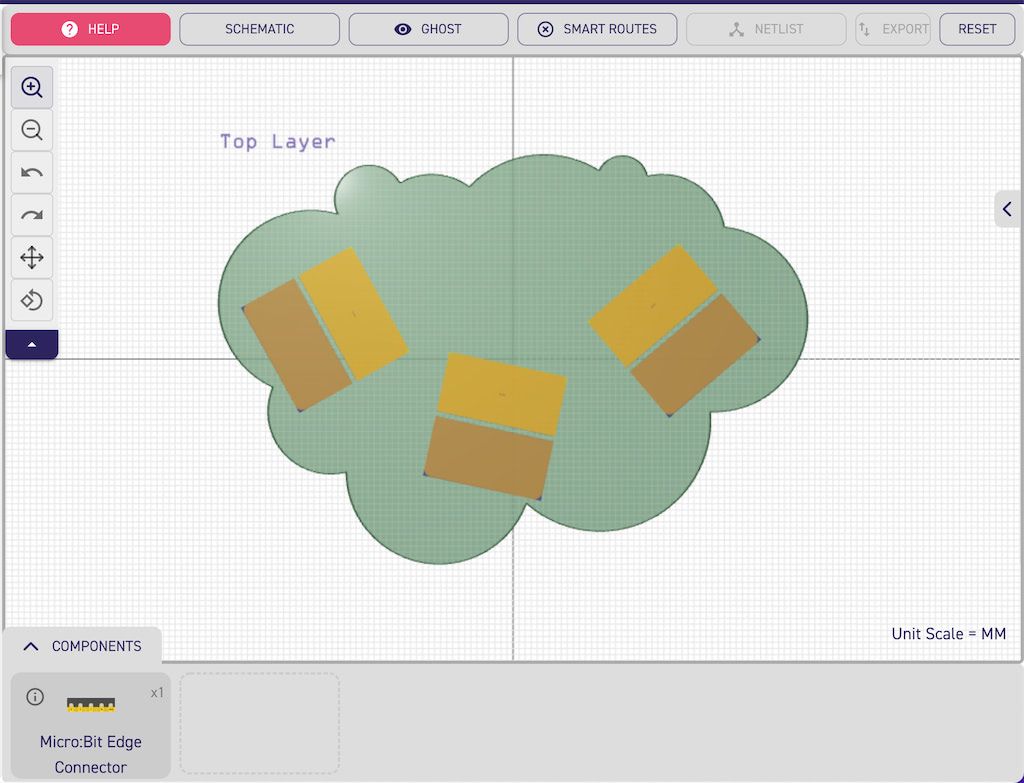
Your circuit has three buttons, so make sure you give each one enough space. If you don't have the placement right the first time, no worries! You can always move or rotate your components!

Hint: use the ghost of the components to help you place them correctly. A ghost is a transparent image of your component, we use them to guide you towards success.

Routing Your PCB#
Routing is a way to connect your components together to create a functional electronic circuit using something we call traces!
Traces can exist in many sizes and it's up to you to select the size that works best for your circuit.
For this circuit you can use whichever size you’d like, but you’ll have more room for component placement if you use the smallest width.
When routing it is always helpful to know where connections need to be made. A schematic, like the one above, is a great way to help you determine how to connect your components most efficiently.
This doesn't mean you need to copy the schematic, in many cases the routes will have completely different paths than the schematic and that is OK, this is your design, have fun with it!

Create Your Traces#
With the trace tool selected from the toolbox in the PCB Editor, click on a pad of the component you want to route.
You'll then be able to drag a blue line that indicates the placement of the trace.
Add A Bend In Your Route#
It's unlikely that all your traces will be straight lines from one component to another. To create an angle in your trace, click on the PCB while using the trace tool.
Routing Considerations#
When positioning a route between components, make sure that the route you are creating doesn't block the way for other routes needed for nearby components.
You may find your layout of a component wasn't ideal and you want to move it, just click Undo and make the layout adjustment.
Routing is an art, use this time to put your own creative twist on what you are designing!
Add a Silkscreen#
 Last but not least is the silkscreen for your PCB.
A silkscreen layer is typically used for marking where components go and adding company logos and product names to a PCB. But, silkscreens can also be used to bring your board to life and make it truly yours.
To add a silkscreen to your board use the silkscreen text tool or the silkscreen draw tool. Both will help create a unique design on your circuit board.